There are still many hidden giants in the electronics and semiconductor industries. The electronic engineering magazine can be frequently encountered at various corporate events and industry exhibitions. For instance, at the two-year, the 600-square-meter exhibition by Keyencehttps://heiautomation.com/ – a comprehensive supplier of industrial automation products, includes core products such as vision/bar code readers, microscopes, static eliminators/safety/sensors, measurement, PLC/engraving equipment, etc. Although the electronic engineering magazine has not conducted a systematic report on Keyence in the past, its presence can always be seen in the list of partners of many semiconductor manufacturers. Even in the market downturn, this company’s annual revenue (net sales) for FY2025 (ending March 20, 2025) reached 10,591.45 trillion yen (approximately 7.061 billion US dollars), with a year-on-year growth of 9.5%; its net income was 3,986.56 trillion yen (approximately 2.658 billion US dollars). The SWOT Analysis evaluates that this company develops innovative automationhttps://www.facebook.com/profile.php?id=100087291657130 products and has made significant contributions to the improvement of global manufacturing efficiency; moreover, Keyence is already at the turning point of factory automation innovation, and keywords such as Industry 4.0, platform automation, and AI integration are all closely related to this company. Additionally, from the financial reports, the company’s operational approach is quite Japanese-style: over 8 billion US dollars in cash flow and zero interest-bearing debt, enabling it to possess extremely strong stability in the face of market uncertainties – this is quite rare in the electronics industryhttps://heiautomation.com/about/.

At the recent 2025 KEYENCE Media Communication Day event, Avy Ruan, the marketing director of KEYENCEhttps://heiautomation.com/, introduced that this Japanese company with a history of over 50 years now has more than 350,000 global customers; not only has it consistently ranked at the top in the Japanese corporate market value rankings year after year, but also its overseas sales in Japan have accounted for more than 60% (as shown in the FY2025 annual report, the overseas sales proportion was 64.81%). KES’s annual report separately lists the revenue of the Chinese region – in 2025, its revenue in China was approximately 1578.91 trillion yen (approximately 1.053 billion US dollars), although it is not the region with the highest revenue for KEYENCE (refer to the domestic revenue of Japan at 3727.53 trillion yen and the revenue of the US region at 1975.79 trillion yen), but as a separately listed revenue region, it is also an important market in https://heiautomation.com/contact-us/KEYENCE’s business map.
Avy mentioned that since the establishment of Keyence (China) Co., Ltd. in Shanghai in 2001, over the past 24 years, it has successively set up 27 branches in 24 cities, “almost all related to the industry have been well covered”. Based on the “direct sales network”, “same-day delivery” and “global support” concepts, such a layout is quite easy to understand. And this media event also gave us the first opportunity to have a preliminary understanding of the technology and products of Keyence. This article is quite lengthy and you can choose to read selectively according to your preference: Part 1: Keyence in the semiconductor industry; Part 2: Introduction to vision systems; Part 3: Introduction to precision measurement products; Part 4: Introduction to microscopic systems; Part 5: Introduction to other sensor products;
The semiconductor business landscape of Keyencehttps://heiautomation.com/contact-us/
Although keyence’s business can be summarized in one sentence as electronic application equipment, from the introduction on its official website, its solutions are targeted at industries such as automobiles, metals, semiconductors/lcd, electronic components, resins, films/papers, food/pharmaceuticals, healthcare, logistics, etc. What we are more concerned about is its semiconductor and electronic applications – especially since keyence’s https://heiautomation.com/about/products and solutions cover all aspects of automated production, from research and development, factory automation, traceability, to logistics and retail, “covering the entire manufacturing lifecycle”. The market data of keyence that can be found in financial reports and public market information is rather limited. Avy, when introducing to the media, mentioned that in the domestic semiconductor field in China, including the main fields such as materials, wafer manufacturing, and packaging testing, all listed companies have cooperated with keyence, accounting for 60%; from the perspective of OEM complete machine factories, this figure is 80%. If the domestic semiconductor market that keyence is involved in is divided into three directions: silicon wafer manufacturing, wafer manufacturing, and packaging testing, from the perspective of performance composition, wafer manufacturing occupies the majority, packaging testing also occupies a considerable portion, while the proportion of silicon wafer manufacturing is relatively small. “It’s not that we are relatively weak in silicon wafer manufacturing – we are proficient in all three directions. This is related to the industry investment situation – since 2020, the investment in wafer factories has been quite significant, so this part of the performance proportion will be relatively higher.”From the perspective of “total OEM transaction coverage”, “keyence has established partnerships with the vast majority of semiconductor equipment manufacturers. In the packaging and testing field, we have business dealings with almost all mainstream enterprises; while in the silicon wafer and wafer manufacturing sector, we have covered most of the major enterprises in the industry, and the scope of cooperation is very extensive. This indicates that keyence has already established a relatively extensive customer base in China – corresponding to the revenue of approximately 1578.91 trillion yen mentioned at the beginning of the text, it is also reasonable. In addition, Avy also mentioned a figure: “In 2024, keyencehttps://studio.youtube.com/channel/UC5jh-_J8N51BACPDqMnnT6Q/videos/upload?filter=%5B%5D&sort=%7B%22columnType%22%3A%22date%22%2C%22sortOrder%22%3A%22DESCENDING%22%7D China will provide over 30,000 service items for semiconductor customers” – each item represents one customer visit, “with an average visit time of 1.5 hours”, so the total annual investment will be approximately 50,000 hours. “This year’s investment volume will be even larger. In this way, we will have a better understanding of the pain points, concerns, and demands of our customers, and can transform them into our experience.” In addition to the “direct sales” globally, keyence can “grasp know-how” and “follow the customers” – “help customers conduct tests, jointly build solutions”, “especially help Chinese customers conduct domestic technology test and verification”, provide “free products and technical support”; all of these have become the advantages of keyence in the Chinese market operation.From a more specific perspective, the current media event of Keyence mainly focuses on introducing its own technologies and products, covering precision measurement sensors, intelligent sensors, flow sensors, vision systems, and microscopic/3D testing systems. Although this is only a small part of Keyence’s existing products, they are all the basis for achieving the aforementioned market share; and based on Keyence’s market position, this is also a good opportunity for us to observe the development level of semiconductor manufacturing automation technology.
Visual system: Distributed throughout the semiconductor manufacturing process
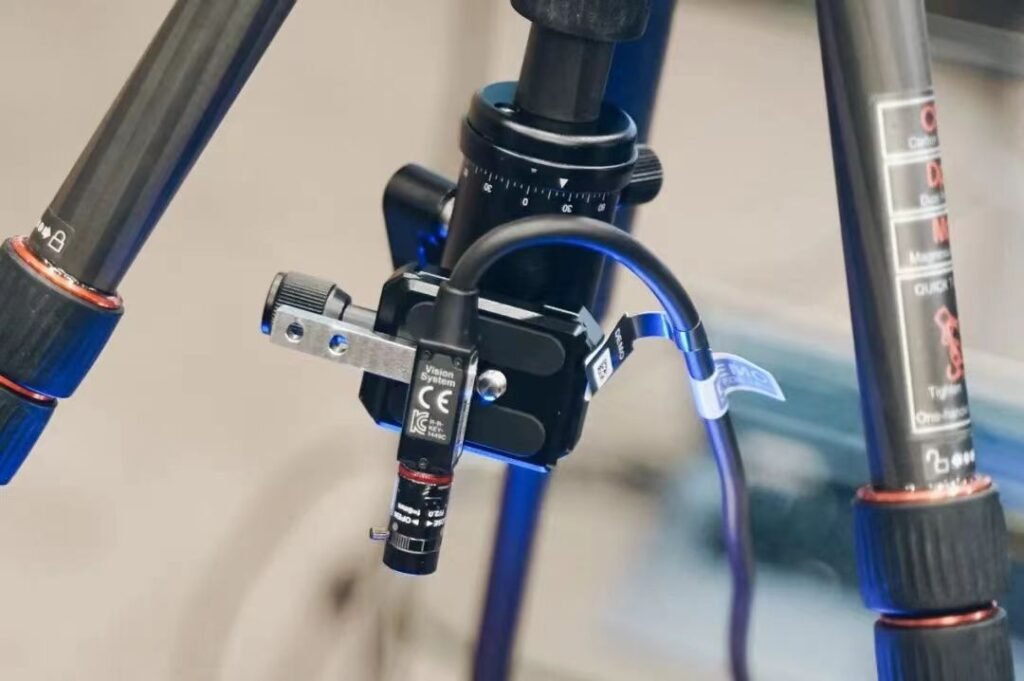
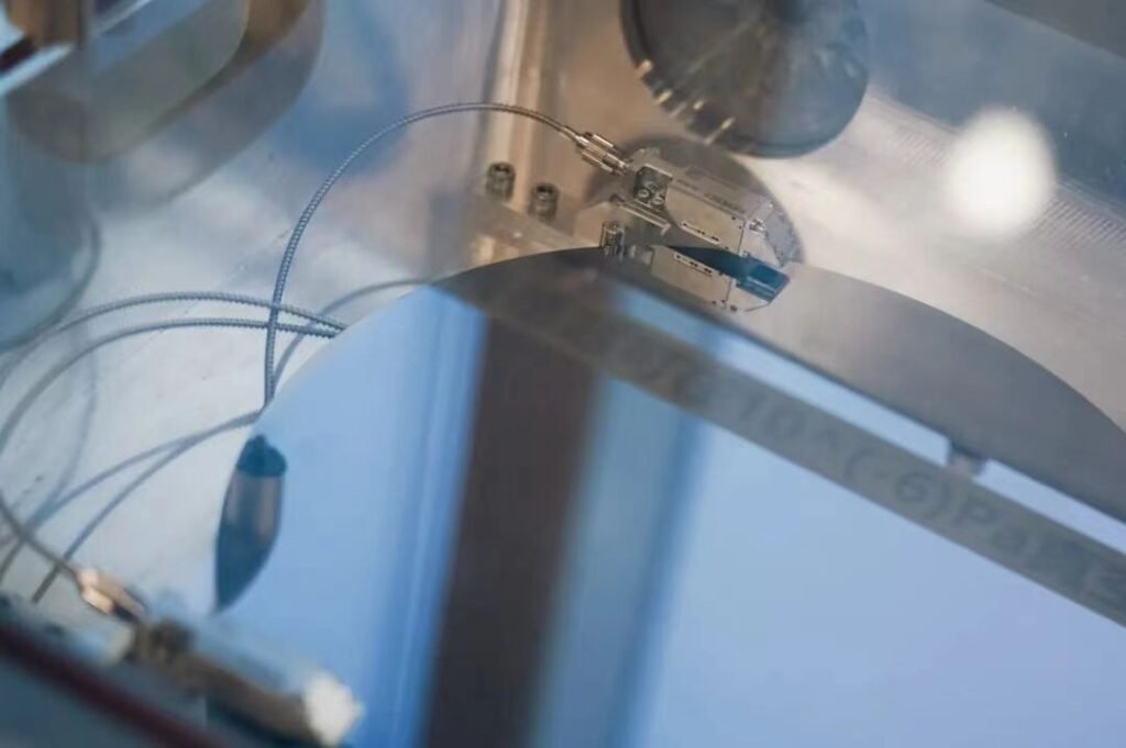
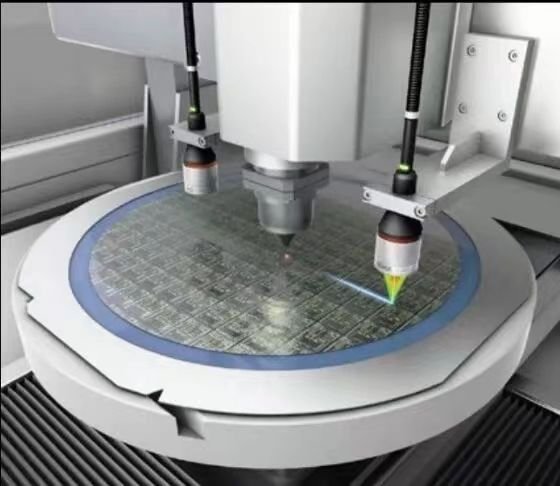
Perhaps for most readers who have some knowledge of Keyence, the aspect that leaves the deepest impression on them is probably its visual sensors and solutions. In the annual report, the company’s president, Yu Nakata, specifically mentioned in his letter to investors the visual sensor that incorporated AI released in the previous fiscal year. At the media conference, Keyence’s introduction of the visual system not only included camera equipment that could be used in the semiconductor production and manufacturing process, but also related to four main application directions implemented through software: positioning, appearance, error prevention, OCR/reading. The term “positioning” refers to the precise positioning of wafers during transmission and in the production process, which is extremely important in processes such as coating, lithography, etching, bonding, etc.; at the same time, for wafers of different materials, “appearance” is also a requirement throughout the entire production process, such as the identification of particles, process scratches, chipping, chamfering, etc.; “error prevention” includes things like Mapping, identification of fragments in the process chamber; “OCR/reading” is naturally the identification of text and reading of codes during transmission, EFEM (Equipment Front-end Module, usually between FOUP and processing equipment), and SORTER (wafer sorting) processes, mainly for querying during quality traceability of wafers. Regarding the camera equipment itself, due to the limited internal space of semiconductor manufacturing equipment, low stability of PC processing – and the problems of confidentiality management, as well as inefficient collection and utilization of data – Keyence engineers mentioned that their camera products have three major advantages:
(1) Small size – The full length of the small camera can reach 6 cm. It is said to be quite rare in the industry and is easy to install, capable of being placed in the processing chamber; (2) Stability – Mainly compared to the PC-connected camera system, the Keyence camera itself comes with a controller and has a significantly faster response speed; (3) Data encryption dongle can be used for production status report management – “It can statistically record data such as inspection status and production quality according to production shifts”; “If there is a problem, it can be quickly retrieved by using the software”; “There is no need to stop the program and data optimization. Real-time updates can be made after offline control.”
Keyencehttps://heiautomation.com/product/ has a visual solution called “2.5DLUMITRAX Line Scan”: “It mimics the human eye, generating 5 different image effects by rotating 8 images 360 degrees, achieving stable detection” – The reason it is called “2.5D” is that “traditional visual solutions can only detect X and Y on a flat surface; our product can detect through 360-degree rotation and lighting, obtaining height information”, so “even when the particle is very small but there is a change in height, we can accurately identify it”. For process wafers, due to the existence of the 2.5D visual solution, even if there are patterns on them (patterns), they can “not be disturbed and detect things like the above liquids and scratches”. Moreover, especially for the edge cracking and chamfering of wafers, the 2.5D line scan can be used, “rotate once, and stably identify the edge cracking on the chamfer”.
One typical application of the visual system is OCR (Optical Character Recognition). For wafer and die, OCR character recognition is not supposed to be a difficult task. However, when it comes to glass sheets, silicon carbide wafers, and bonding process wafers (bonding wafers), various practical problems may arise: including the reflection issue mentioned earlier; and “the bonding patterns are all different”, sometimes there may also be residual substances from the previous step. OCR then faces varying degrees of interference – https://www.instagram.com/sunny.zeng5/Keyence’s AI OCR technology can accurately recognize characters while also “helping customers improve the process at an early stage”. Additionally, in addition to reading codes, AI OCR applications can also “ALIGNER find edges and position” – “Previously, Aligner needed two devices to complete edge finding and code reading, but with our one camera, we can accomplish both tasks”. This saves space and costs.
Precise measurement: The thickness and warpage of the wafer must also be measured.
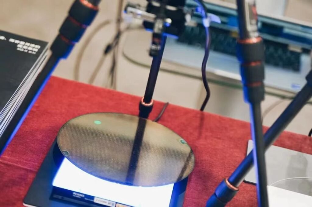
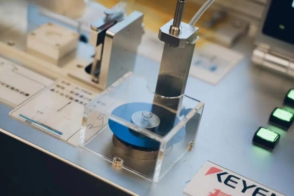
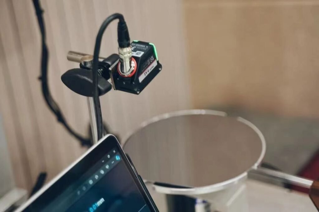
Keyencehttps://heiautomation.com/product/ has a business segment that places greater emphasis on high-precision and high-speed measurement – precision measurement. Typical products include the color laser coaxial displacement meter CL-3000 series – with a compact size, it can perform high-precision position measurement in vacuum and high-temperature environments. It is said that this is a sensor product specifically designed for customers in the semiconductor industry after clearly understanding their needs: “It can capture changes such as mechanical hand vibrations, minor misalignments, and wafer warping with sub-micron accuracy.” Specific applications include, for example, position and tilt detection of the coordinate table during lithography processes, focusing during direct exposure, and position and tilt detection of the loading table in a vacuum environment; as well as height measurement of robotic arms in a vacuum environment for PVD/CVD/ALD devices, and wafer warpage measurement, etc.
This product adopts a split design, consisting of a sensing head and a controller. Its basic principle is that the colored laser passes through the polarization-preserving optical fiber to reach the sensor probe. Inside the probe, there is a set of diffraction lenses – which focus the colored laser according to its wavelength at different heights. Based on the principle of spectral confocalhttps://heiautomation.com/product/ imaging (only the light at the focal point can be effectively received), “only the light focused on the surface of the object can return through the lens to the common focal pinhole and back to the spectrometer – the spectrometer splits the reflected light and projects it onto the CMOS sensor according to different wavelengths.” For example, to measure the thickness of a piece of glass, the reflected light focused on the surface of the glass is received and the wavelength of the reflected light is identified to confirm the position of the upper surface; the light continues https://heiautomation.com/festo-cylinders-versatile-applications-across-various-industries/to penetrate the glass and the light focused on the lower surface is reflected, and the wavelength of the reflected light can also be identified in the optical unit to confirm the position of the lower surface; the distance between the two is the thickness value of the glass. To achieve high-precision measurement, we also need to add correction coefficients such as refractive index to ensure ultra-high precision detection. The main advantage of the CL-3000 lies in the colored light source – based on laser excitation of the fluorescent material to emit light, compared to the traditional white LED light source, the wavelength band that can emit light with high brightness is wider, so sufficient light can be received at different positions, “our product has a longer lifespan and is more stable”; on the other hand, compared to the triangularhttps://heiautomation.com/about/ reflection scheme, spectral confocal itself also has principle-based advantages, “regardless of close or distant distance, the size of the focused light spot remains unchanged, and the measurement value is more accurate.” These two characteristics also enable the CL-3000 to be applicable to different materials such as metal surfaces, black rubber surfaces, mirror surfaces, glass surfaces, gel surfaces, etc., while still ensuring high precision.
Additionally, as mentioned by the engineers from Keyencehttps://heiautomation.com/about/, this color laser coaxial displacement meter features a small size and excellent environmental performance. Due to its split design, the sensing head itself is small enough, and the optical path design can utilize a 45° turning mirror, allowing for installation in various directions, saving Z-axis space – for example, in probe stations. At the same time, “the sensing head can be used in vacuum, high-temperature, or electromagnetic-sensitive scenarios – it does not generate heat itself, which is beneficial for controlling environmental variables such as the temperature control of semiconductor manufacturing equipment.” “It can be used for a long time at 200°C, with precision maintained at the sub-micron level; when paired with a dedicated feedthrough flange and connected using a connector, it enables vacuum measurement, and maintenance is simpler; during shipment, it undergoes vacuum drying treatment, allowing for direct opening and installation in the customer’s cleanroom without the need for secondary dust removal.” Part of the reason for its excellent environmental performance is that the CL-3000 does not use organic adhesives, and “the components use zirconium oxide materials, which do not cause any leakage when placed inside the probe.” In the direction of precise measurement, another product introduced by Keyence https://heiautomation.com/contact-us/at the media event is the spectrophotometric wafer thickness gauge SI-F80R, specifically designed for measuring “wafer” thickness. It is said to be widely used in CMP equipment, for example, during the backside thinning process, this sensor is needed for monitoring the thickness of the wafer (the so-called NCG non-contact precise thickness measurement); and it is also used for measuring wafer flatness, mask plate positioning, etc…
“This sensor uses a special light source that can penetrate semiconductor materials such as silicon, indium phosphide, gallium arsenide, and silicon carbide; and the light spots are very small, with a diameter of only 25 μm. Even after lithography has been completed and a circuitry wafer has been https://www.youtube.com/@%E6%9B%BE%E6%85%A7%E5%A9%B7-z6j/shortsproduced, it can still perform stable measurements without being affected by the patterns.” “It can measure 5000 times per second, with a very fast sampling speed.” “The measurement accuracy is up to 60 nm.” Its basic principle is to use a near-infrared SLD light source (super radiative light-emitting diode), which emits wide-bandwidth light. Some of this light is reflected from the surface of the wafer, and the other part penetrates the wafer and then reflects again – these two reflected beams interfere within the probe”, forming an interference spectrum; by analyzing the phase difference or light intensity distribution of the interference fringes, the thickness of the wafer can be obtained.
Microsystem: Capable of observation, measurement, and element identification
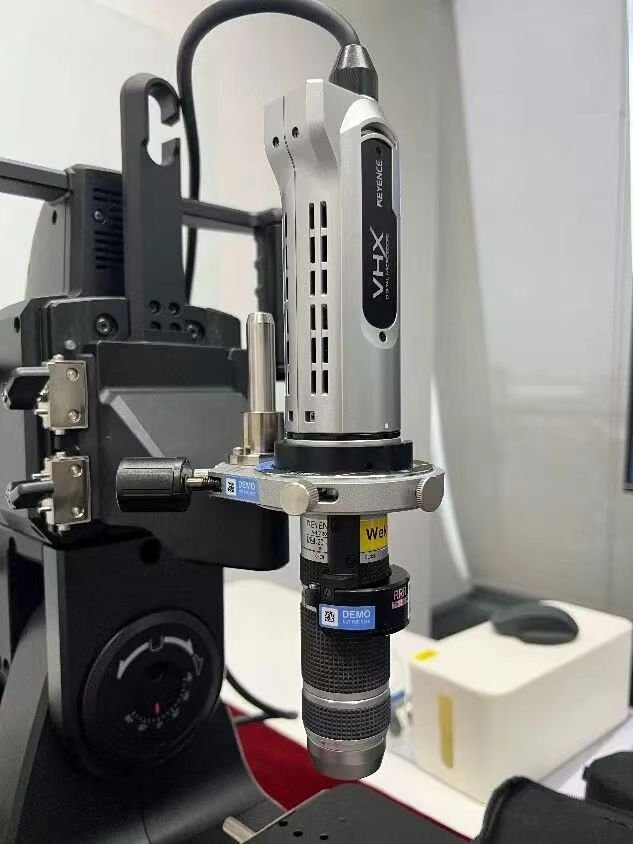
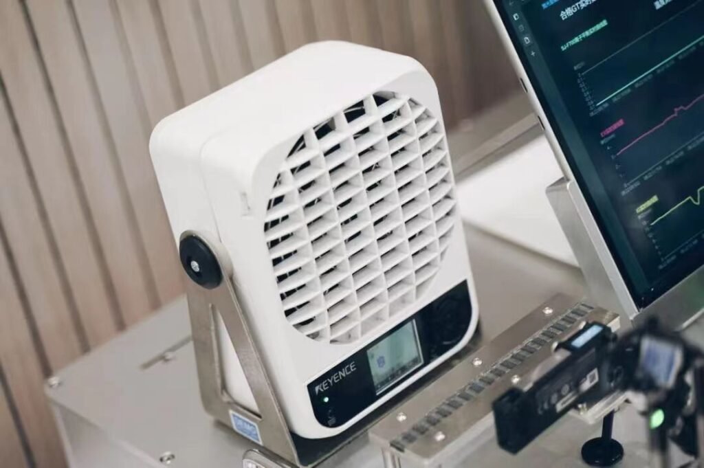
Another aspect that impressed us during the media presentation was its micro/3D testing system – especially considering that Keyence has a long history in the field of digital microscopes. The engineer explained that the micro/3D testing system belongs to Keyence’s https://heiautomation.com/“offline” products – compared to the “online” products used directly on the production line, the “offline” equipment is used by quality and quality control departments or testing rooms. The main product introduced by Keyence this time is its digital microscope VHX-X1 series, which is already its “6th generation” by 2024. This series has a significant feature: platformization, supporting various analysis tasks. Previously, body microscopes, metallographic microscopes, electron microscopes, measurement microscopes, and elemental discrimination machines were independent products; through platformization, “the effects that required 5-6 devices before could be achieved with just one device: higher completeness and cost reduction can also be achieved.”
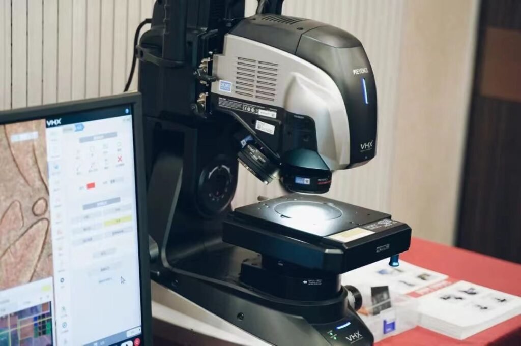
Here, we will discuss the features of this series of products from three aspects: observation, measurement, and element discrimination. (1) In terms of low-magnification observation, engineers from Keyence stated that their products have the characteristic of “extremely large depth of field” – that is, a larger clear observation range in the depth direction. For example, when observing the pins and solder joints of a chip, there is less blurring of the pins. In low-magnification observation, the depth of field range that the VHX-X1 microscope can achieve (seemingly within 20x focal length) is “more than 20 times that of ordinary optical microscopes on the market”. We also asked the engineers from Keyence https://heiautomation.com/on-site about how their microscope products achieve such an extremely large depth of field. The engineers said that in addition to the optical design (16 lenses in 4 groups), there is also “post-processing adjustment”. “In the case of a relatively small lens magnification, a balance is found between resolution and depth of field, ensuring basic resolution while retaining the characteristic of a large depth of field.” Additionally, Keyence’shttps://heiautomation.com/ digital microscopes also support handheld and multi-angle observation, “allowing for direct image collection at the scene”; “the lens supports a 90° tilt on both sides – rather than only being able to observe in the vertical direction; combined with the horizontal rotation of the stage, a 360° observation can be achieved.” In high-magnification observation, Keyence provides a “depth of field synthesis” function at the software level: “By driving the lens with a motor, scanning from below to above, retaining clear images at different positions (focus plane), and finally synthesizing a large-depth-of-field image”, ensuring that the final imaging is almost clear everywhere; at the same time, by recording “position changes” – it is speculated that this combines the position record of the focusing motor, “combined with our unique algorithm, a surface 3D topography map can be generated, facilitating users to make a preliminary judgment on surface defect issues”; and it can also provide size information such as the height of the device.Apart from depth-of-field synthesis, due to the small field of view for high-magnification observation, Keyencehttps://heiautomation.com/about/ has also developed “an ultra-large micro-platform specifically designed for 12-inch wafers”, which enables the capture of a 300x300mm full-area high-precision image in a single photo by moving the platform and image stitching; “The image can capture up to 10 billion pixels”. (2) Regarding measurement, the VHX-X1 series microscopes support two-dimensional size measurement, three-dimensional size measurement and roughness analysis, as well as particle analysis or cleanliness measurement using custom modules – “A standalone cleanliness analyzer itself is very expensive, but our microscopes only need hardware installation and software integration to achieve such functions”. This also reflects the “platformization” feature of this series of microscopes. The engineers also particularly emphasized that Keyence’s digital microscopes support “one-click automatic calibration”. Compared to the inefficient process of having specialized personnel bring tools to the site for calibration 2-3 times a year, “Keyence’s products can achieve all magnification levels of re-calibration simply by clicking the software, without the need for manual operation and hardware installation”. “It’s fast, taking about 2-3 minutes to complete”; “The results can be output and saved, generating a measurement report for the customer, which also has credibility”; “Of course, there are international certificates to ensure its accuracy”. In terms of efficiency in observation and measurement: At present, Keyence’s digital microscopes support “automatic focusing”, “After enabling this mode, when the observation/measurement object moves, there is no need to frequently press the automatic focusing button. The motor can automatically find the focal plane”; Additionally, it supports “fast replay”, in scenarios requiring repeated measurements, “The first measurement record template, the next time only needs to call the template, without manual operation, the results can be automatically output”, “This significantly improves the efficiency of repetitive work”.
(3) Element discrimination is another distinctive feature of the VHX-X1 series. It enables “element discrimination to be carried out simultaneously while observing”. This is reportedly quite rare in the entire industry. Firstly, the foreign object is identified through the microscope itself, and then “click the button to automatically launch the element discrimination module (EA-300), locking the position observed by the microscope”; directly in the air, “it only takes about 1 second to identify the elements of the characteristic object”. Unlike traditional solutions, where the foreign object needs to be found first and then removed using tools, and elemental discrimination is done using conventional elemental analysis methods. “In the semiconductor field, it is commonly used for foreign object detection”: “When foreign objects are involved in the production process, to determine the type and origin of the foreign object, our microscope finds it and discriminates the element type, which can assist in determining which process or step it was produced in, thereby improving work efficiency.” The engineers of Keyencehttps://www.facebook.com/profile.php?id=100087291657130 also listed cases where the VHX-X1 digital microscope is used for IC graphic observation, wafer surface defect observation, concave and convex observation level SEM effect observation, photomask size and area measurement, packaging gold wire observation and measurement, probe test after damage appearance and depth measurement, and surface foreign object element discrimination, etc. Due to the length limit of this article, we will not delve deeper.
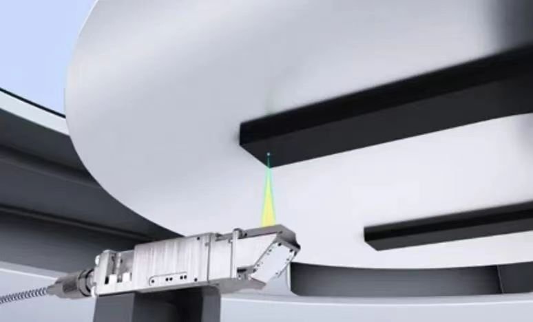
Clamp-on ultrasonic flowmeter, along with more sensors.The media will provide two additional key points at the event, namely the clamp-type ultrasonic flowmeter and the intelligent sensor – it seems that they were not presented according to their 9 major business directions. This article will present these sensors last for a comprehensive and brief introduction – they also play an important role in the semiconductor manufacturing process. Flow sensors are also one of Keyence’s https://www.facebook.com/profile.php?id=100087291657130flagship products. This time, Keyence introduced us to the FD-X series clamp-type ultrasonic flowmeter. On the one hand, as an “external clamp” flowmeter, “it doesn’t require pipe rupture”; on the other hand, the ultrasonic flowmeter has two parts in principle – the emission and the reception, which are usually arranged diagonally. Ultrasonic waves travel in the direction of the current flow or the opposite direction, and their speeds will increase or decrease, and the measurement is based on the difference in propagation time for flow rate conversion.

The engineer mentioned that the advantages of the FD-X series include stable detection, zero pressure loss, and easy installation. At the same time, it also performs well in terms of resistance, high-temperature resistance, bubble detection, and repeatability accuracy. This clamp-type ultrasonic flowmeter is used in silicon wafers, wafers, and chip factories. After all, “liquids are everywhere.” “From EFEM to the process end, such as cleaning, furnace tubes, thin films, equipment including UV curing and developing equipment, and CMP, ion implantation equipment, etc., will all use liquids to some extent, and all require flow detection.” “For example, in process machines, cooling water or some liquid solutions are needed; these liquids enter from the auxiliary unit or industrial system; the liquid in the industrial system is then transported from the plant management end; and finally, the waste liquid is discharged… The entire process cannot do without liquid flow detection.” Specifically, single wafer cleaning equipment (single clean), liquid solution mixing, wafer surface pure water cleaning, backside cleaning, drying with isopropyl alcohol, etc., all require flow detection – in this process, some customers need to detect the tiny flow of acid solutions and have requirements for instantaneous flow rate – using the FD-X series from Keyencehttps://www.youtube.com/@%E6%9B%BE%E6%85%A7%E5%A9%B7-z6j/shorts, enabling the minimum flow mode can solve the problem.

For instance, in the coating (applying photoresist) and developing (developer) equipment, there might be specific requirements for the amount of photoresist dispensed. With the help of FD-X, the amount of photoresist dispensed each time can be monitored, and high precision can be achieved. “This easily resolves the issues of retraction of photoresist and bubbles affecting its accuracy”. Also, monitoring the flow rate of the developing solution, as well as pure water cleaning, cooling water management, and plant-side liquid transportation, all have flow rate monitoring requirements. In the CVD/PVD/ALD process, vacuum pumps and reaction tanks require cooling water, and in addition, the liquid transportation on the plant side also needs to use flow sensors. It is said that a customer has completed the pipeline design for the PVD process and cannot stop the machine to install a flow meter. They chose to adopt the external clamp solution from Keyence to solve the installation problem. Besides, in the direction of intelligent sensors, Keyencehttp://www.heiautomation.com has introduced several products, including ESD static solution and measurement sensors. Among them, the fan-type static eliminator (typical such as SJ-F700 series) is a quite interesting product.
These products are designed to address the issue of static electricity: depending on the amount of charge carried by the product, it releases the corresponding negative charge if it has a positive charge, and vice versa. The electrode needles, by applying high voltage electricity, ionize the molecules in the air, generating positive or negative ions, which neutralize the surface charge of the target object to eliminate static electricity. The engineers mentioned several features of this series of products: (1) “The electrode needles will automatically clean with a brush before the equipment starts – it can be done regularly for cleaning”, eliminating the trouble of manual maintenance; (2) The display screen can show and monitor the charge of the target object; (3) The air flow can be adjusted from 1 to 7 gears, with the maximum distance being 3 meters in front and 1.5 meters left and right; (4) There is an option for a small fan, only the size of a business card; there is also a long-shaped one suitable for a wider range of static elimination; (5) It can achieve ±1V balance (the degree of charge balance between positive and negative ions). There is also a long “ion wind stick” type product, such as the SJ-M series small wind stick suitable for limited installation space, the SJ-H series wind stick with replaceable single-crystal silicon material to achieve ISO Class 2 cleaning level, and the SJ-E series that saves compressed air and is more cost-effective; and the SJ-LM series “nozzle type static eliminator”, which can be used for static elimination in processes such as post-chip testing, based on light to clearly indicate the working state, and multi-directional adjustment for a 360° full range of static elimination; there are also handheld air guns, static measurement instruments, etc.

For wafer position detection and rough calibration, Keyence has sensors such as the beam-type sensor (IG series) – based on the notch holes or flat positioning edges of the wafer itself. “The beam-type sensor has a light curtain. When the wafer rotates into the light curtain, collecting edge data can confirm its position.” Moreover, even when applied to vacuum environments of different processes, this series of sensors also support detecting wafer positions through quartz glass. Its accuracy can reach “within 4 seconds, for 8-inch flat-edge wafers, the X and Y directions of the position are less than 0.1mm, and the θ direction is less than 0.1°”. Other sensors have a simple overview: The EX series eddy current sensor – with the size of a small finger, can detect various axis vibrations relatively flexibly (by sensing the vibration amplitude to confirm the operation status of the equipment), and in devices such as bonding/soldering equipment, perform repeated precision detection (to confirm the relatively accurate installation requirements of the mechanical structure); The FW series ultrasonic sensor can detect the liquid level height in wet processes, and confirm whether the wafer is in place in devices such as cleaning machines – mainly for some scenarios where the precision requirements are not so high, and infrared methods may have an impact on the circuit.
The IV series intelligent image sensors can be used for wafer character OCR detection – “After AI illumination and AI photography, followed by serial number detection and reading”, especially “compatible with the common SEMI dot matrix fonts in the semiconductor industry”, and as mentioned in the visual system introduction, they have excellent and stable support for patterns, transparent materials, SiC wafers, etc.; They can also be used to detect whether there are slanted, bent, or stacked wafers in the FOUP wafer box, “One sensor is placed on each side of the wafer box, and it slides up and down using a slide rail”, “Stable detection of these issues through image shooting”; The IL series laser displacement sensors, commonly found in EFEM’s robotic arms, mainly perform repeatability accuracy detection, “Three sensors are set in the X, Y, and Z directions, and continuous 48-hour collection is performed to detect whether there are repeatability accuracy problems”, combined with a data acquisition instrument to automatically generate tables, and no manual operation is required during the process: If there are problems, they can be traced and improved, and it is said to have a very good sales performance among robotic arm manufacturers; The GT2 series contact measurement sensors, in the wafer thinning process, use a contact measuring pen to measure the thickness of the wafer; The minimum force applied can be 0.1N, and a resin head can be replaced without causing damage; During the silicon wafer manufacturing process, this series of sensors can also be used to measure the thickness of the silicon wafer, with a minimum applied force of 0.2N and a maximum repeatability accuracy of 0.1μm… In addition, there are also vacuum environment robotic hand positioning, wafer temperature measurement, etc., but due to the length of the text, more details will not be covered.
Interested readers can visit the website of Keyence to see their solutions in the semiconductor field. The above-mentioned are just the tip of the iceberg. However, from the introduction of these different products and solutions – especially in terms of vision, microscopic systems, and the specific applications of different products in the semiconductor manufacturing process – apart from the sensors and hardware equipment themselves, the significant investment made by Keyence in the overall solution lies in the software. For instance, the judgments in different applications and scenarios of the vision system, the depth-of-field synthesis, image stitching and detailed presentation of measurement data in the microscopic system, as well as the sensing assistance of precise measurement and more sensor solutions in the manufacturing process, all require a considerable accumulation of software and algorithms. Furthermore, “Keyence’s advantage is not only the products themselves, but also our experience.” “Keyence has been in contact with and invested in the semiconductor industry earlier than its peers. We have many mature cases that have been truly implemented on the ground.” From the specific cases mentioned by the engineers when introducing different products and the clear indication of which aspects and scenarios these products have solved, it can be seen. Among the several Keyence engineers during the product introduction process, the word “operational rate” was mentioned multiple times. It is clear that semiconductor customers highly value operational rate and require “no downtime” or “as little downtime as possible”. After all, this involves productivity and cost investment. It is believed that Keyence’s long-term accumulation in the global semiconductor manufacturing field, as well as its communication and collaboration with customers, are the basis for its continuous investment in “operational rate”, enabling all products to evolve towards improving operational rate.
“We want to bring these experiences to the Chinese semiconductor industry and contribute to the development of China’s semiconductor sector,” Avy said. At the same time, by leveraging Keyence’ global experience, “with the help of overseas branches and domestic technical team members, we can jointly support Chinese customers in better going global.” At the same time, we will also expand Keyence’ larger market in the field of process automation.”