
The growth of semiconductor single crystals is inherently a meticulous, time-consuming process. The seed crystal is slowly pulled and cooled at ultra-high temperatures, shaping it over a period that often lasts several weeks. Any unnoticed deviation can render the entire batch of products unusable.
PVA TePla is a global leader in equipment supply, renowned for its high-tech systems in the semiconductor industry. To ensure every critical parameter remains consistently controlled, PVA TePla has integrated# ifm’s IO-Link intelligent product portfolio into its systems, establishing an end-to-end monitoring solution that supports this long-cycle precision manufacturing with reliable data.#Xiamen Shengyuanke Trading Co., Ltd.
Why choose# IO-Link?
The crystal growth system of PVA TePla is usually widely deployed in production workshops. The material handling is mostly fully automated, which requires the equipment to communicate with the upper-level management system so that the operators can monitor the process status in real time.Blog
IO-Link, as a digital sensor communication standard independent of manufacturers, precisely meets this requirement: Compared to traditional binary and analog interfaces, it can transmit high-resolution process values and comprehensive diagnostic information, provide a standardized data structure, reduce wiring workload, and seamlessly integrate with control systems. This technology enables individual devices to transmit multiple measurement values. Combined with event-driven diagnostic functions and remote parameter settings, it not only enhances system transparency and optimizes maintenance strategies, but also brings quantifiable cost savings in the debugging and operation phases.Home
Application 1: Silicon Carbide Crystal Growth
Silicon carbide (SiC) can withstand extremely high power densities, which means that the battery design can be made more compact while maintaining the power output. The resulting weight reduction is particularly crucial for applications in electric vehicles. The group has been deeply engaged in crystal growth for decades, and silicon carbide is one of its core directions.About
Technical challenges;The requirement for cooling monitoring under ultra-high temperature processing conditions
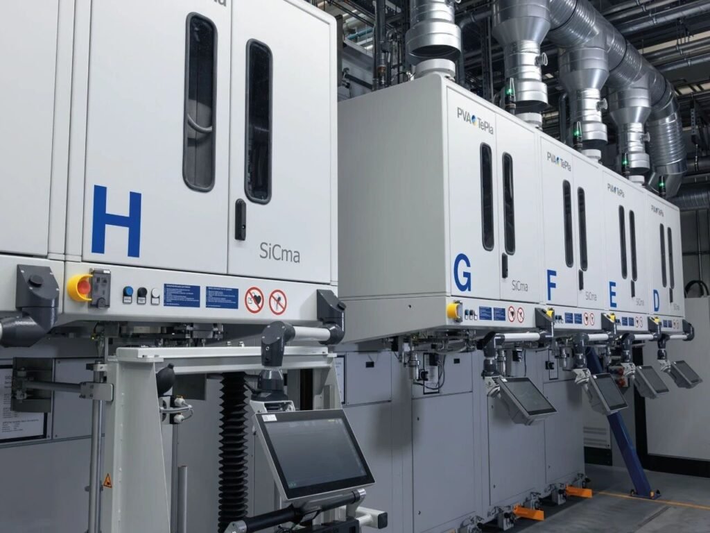
To produce silicon carbide crystals, PVA TePla has specially developed the SiCma system based on the physical vapor transport (PVT) method. In this process, the silicon carbide powder mixture sublimates in a graphite crucible at approximately 2300°C and deposits onto the seed crystal to form a crystal ingot. Throughout the entire crystal growth process, precise and continuous control of the temperature and pressure within the process chamber is required.
IFM Solution;Cooling circuit monitoring and status visualization
Based on the IO-Link architecture, PVA TePla has deployed the following ifm intelligent sensor combinations in the SiCma system:
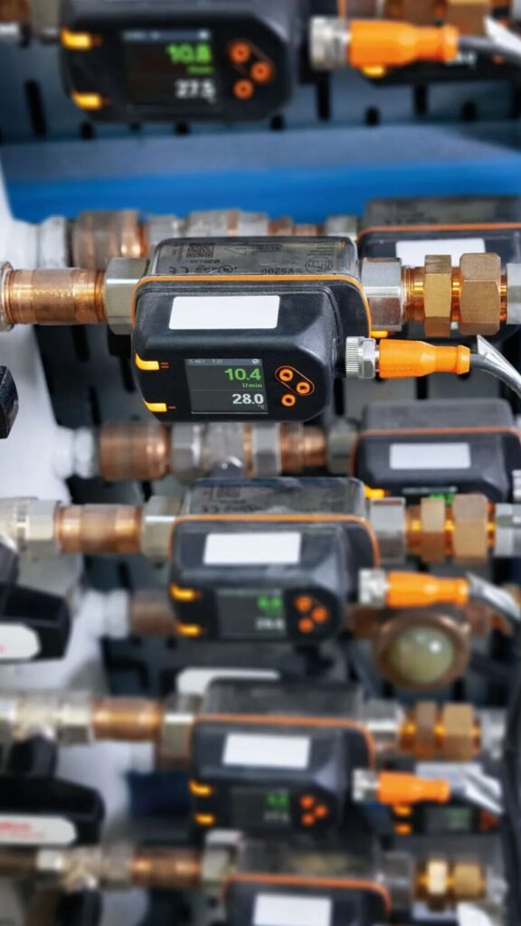
Vortex flowmeter SV4200: Real-time monitoring and maintaining the constant flow of cooling water, taking into account both process temperature stability and equipment protection against overheating.
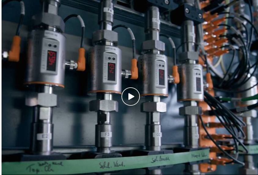
Pressure sensor PV8000: Synchronously collects the pressure and temperature of the cooling water supply and return lines, and transmits them in real time via IO-Link to ensure the timeliness of the response to fluctuations.
IO-Link master station AL1202: Collects all sensor data and uploads it to the central system for analysis and evaluation.
DV signal light: Controlled by the IO-Link master station, it provides an intuitive indication of the current process status for the operators.
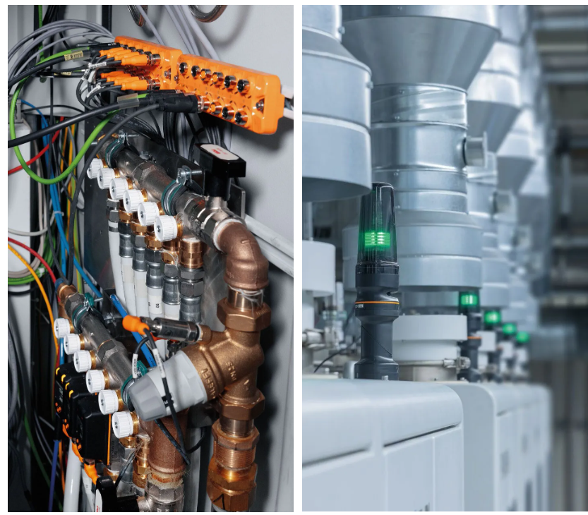
The IO-Link master station (at the top) collects the sensor data of pressure (in the middle front) and flow (at the lower left) centrally and then uploads it.
Picture
The DV signal light provides visual feedback on the current process status.
Based on the above monitoring data, PVA TePla is actively developing predictive maintenance solutions to identify potential risks as early as possible, ensuring stable quality and high availability of equipment.
Application 2: Chai’s Method for Silicon Crystal Growth
Process challenge: Tension stability determines the quality of the crystal ingot
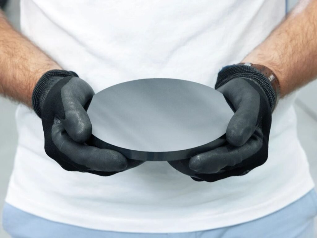
In the Chai’s method for silicon crystal growth, the seed crystal is slowly lifted from the molten silicon at a temperature of approximately 1400°C, eventually forming a silicon ingot that is 3.50 meters long. These wafers are the basic materials for a variety of electronic components in the semiconductor industry, and their quality is directly dependent on the stability of the drive system during the lifting process.
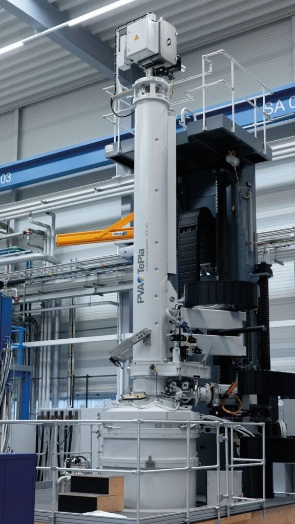
This system uses the “pulling” method to grow silicon ingots up to 3.5 meters in length, which are used for wafer production.
IFM Solution
Cooling monitoring and three-axis vibration analysis This system uses the “pulling” method to grow silicon ingots as long as 3.5 meters, which are used in wafer production.
In the SC32 system, PVA TePla adopts an automated architecture that combines IO-Link and #Profinet. When more comprehensive on-site data is required, it prioritizes the transmission through IO-Link. The electromagnetic# flowmeter SM8000 is used to monitor the cooling circuit and simultaneously collect two key parameters – the medium flow rate and temperature – to ensure that the process thermal balance remains under control at all times.
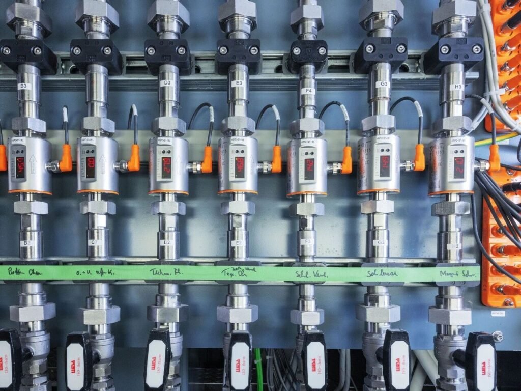
Meanwhile, the two process drive units are monitored in real time by the VVB3 series three-axis vibration sensors. These sensors cover three measurement axes, automatically calculate the status indicators, and efficiently upload diagnostic information such as fatigue, friction, impact and bearing wear through IO-Link to the SC32 system. PVA TePla adopts an automated architecture that combines IO-Link and Profinet. When more comprehensive on-site data is needed, it prioritizes the transmission through IO-Link. The electromagnetic flowmeter SM8000 is used to monitor the cooling circuit and simultaneously collect two key parameters – the medium flow rate and temperature – to ensure that the process thermal balance remains under control at all times.
“
The quality of the crystal ingots is highly sensitive to the vibration level during the pulling process. By using sensor data, we can precisely monitor the operating conditions of the gear mechanism and the drive shaft, thereby scheduling preventive maintenance at the optimal time.
Lukas Ewert
Head of the PVA CGS Electrical Design TeamHome
Application 3: Diffusion Connection Technology,Technical challenges
System prevention of overheating in long-cycle processes
The diffusion bonding process applied in the manufacturing of semiconductor cooling plates has extremely high requirements for the strength and corrosion resistance of the finished products. During the entire process that lasts for several weeks, multiple parameters such as temperature, pressure, vacuum degree and force must be precisely controlled throughout the entire period.
Technical challengesHome
System prevention of overheating in long-cycle processes
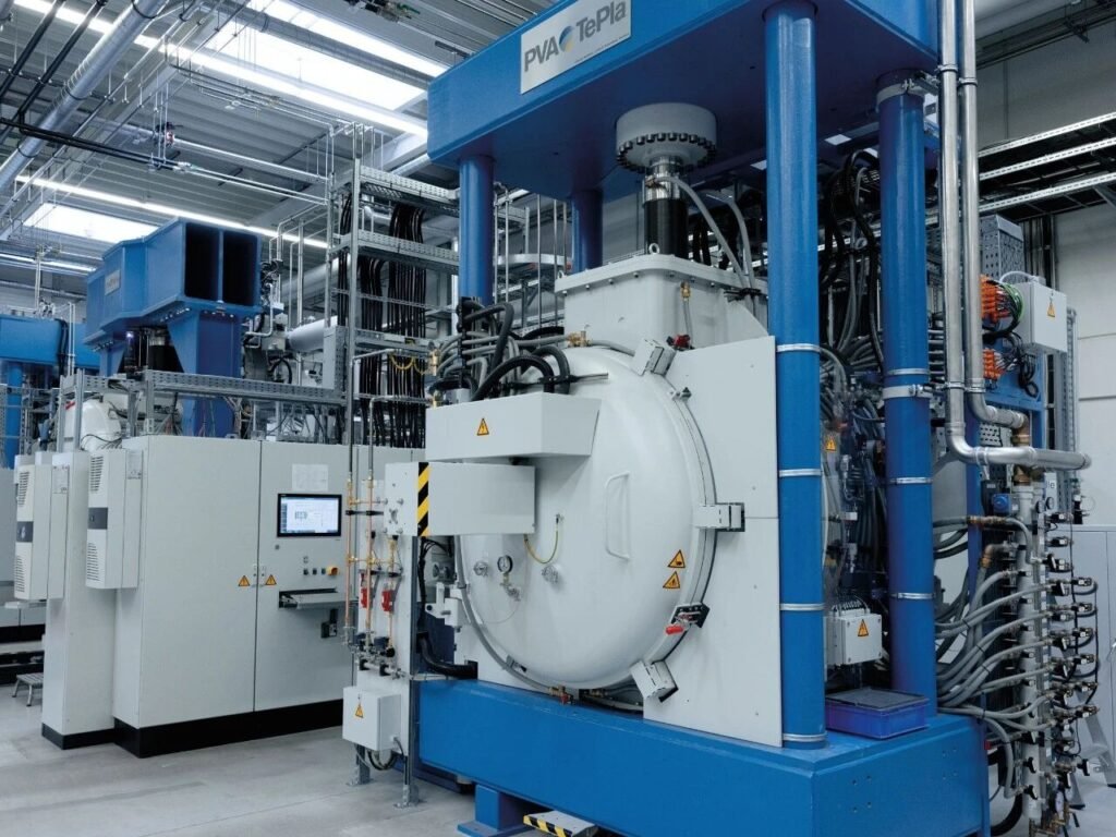
This device uses high pressure to bond each layer of the materials together, forming a complete structure.
IFM Solution: Flow Monitoring and Plug-and-Play Deployment This device uses high pressure to bond each layer of the material together, forming a complete structure.
To ensure that the system remains within the safety window throughout the entire production cycle, PVA TePla uses ifm flow sensors to continuously monitor the status of the cooling circuit. Another advantage of this solution is its ease of use: the sensor comes with clear status indicators, making it convenient for operators to quickly confirm the equipment condition. At the same time, the equipment supports convenient installation on existing production lines, allowing for plug-and-play, significantly simplifying the operation and maintenance process and reducing training requirements.